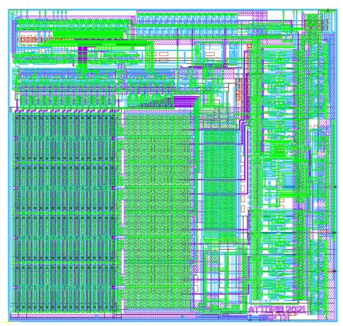
Latest Attopsemi I-fuse OTP Memories Based on Ground-Breaking New Architecture Now Available on X-FAB’s 180 nm Technology
Tessenderlo, Belgium and Hsinchu, Taiwan – May 10, 2022
X-FAB Silicon Foundries, the leading analog/mixed-signal and specialty foundry, together with Attopsemi, the innovative one-time programmable (OTP) IP solutions provider, today announced that the latest version of Attopsemi‘s I-fuse® IP with its next generation architecture has been successfully demonstrated on X-FAB’s XH018 180 nm process technology. It is available in different memory densities, ranging from 512 bits to 8 KBytes, with several customer projects already being ramped up to volume production.
Attopsemi‘s pioneering new I-fuse S3™ architecture means that the area taken up by the IP is at least 50% less compared to previous versions, without trading off program window range, program voltage and any of the numerous other benefits associated with the original. This enables a dramatic reduction in OTP footprint, as well as a decrease in peak and average current consumption by between 1/3 and 1/2, while still keeping to a 3.3 V standard I/O voltage for programming.
X-FAB’s XH018 is a powerful modular sensor and high-voltage EPI technology, specifically intended for addressing a wide variety of prospective customer scenarios. This technology supports an extended temperature range from -40 to 175°C and a modular 1.8 V/3.3 V ultra-low noise process with a multitude of different automotive-grade non-volatile memory options. Attopsemi’s I-fuse® solution is an optimal fit for X-FAB’s expansive memory portfolio, complementing the company’s current NVM offering. The incorporation of I-fuse® into XH018 will extend the reach of this process into various industrial, medical and consumer applications where 3.3 V operation coupled with compact and cost-effective dies are called for.
“We are pleased with the performance of the XH018. The high reliability of this X-FAB process has resulted in first-time-right integration,” states Shine Chung, Chairman of Attopsemi. “It is very encouraging to see that our collaboration has already triggered new projects with common customers in industrial and consumer areas, and is starting to open up new opportunities throughout the medical sector too.”
“This latest I-fuse® implementation further adds to our successful story of collaboration with Attopsemi. Aligned side-by-side with the present X-FAB proprietary NVM portfolio, the Attopsemi IP solution is broadening the target applications. It presents our customers with an optimized die cost, via the combination of no additional mask layers on top of the XH018 core, plus the footprint reductions that the new architecture enables,” adds Nando Basile, Product Marketing Manager for Memory Solutions at X-FAB. “We now have an increasing number of products where I-fuse® has been embedded, with transitioning to mass production already underway on specific 180 nm and 130 nm platforms.”


